
Scanning Electron Microscope Laboratory
The Scanning Electron Microscope (SEM) Lab is located in Room 2-17 of the Earth Sciences Building. This facility is open to all University of Alberta researchers, as well as researchers from other universities, government agencies, and industry. Technicians are available for instrument operation, alternately users from the U of A may be trained to operate independently and run their own samples.
Our Equipment
Zeiss Sigma 300 VP-FESEM
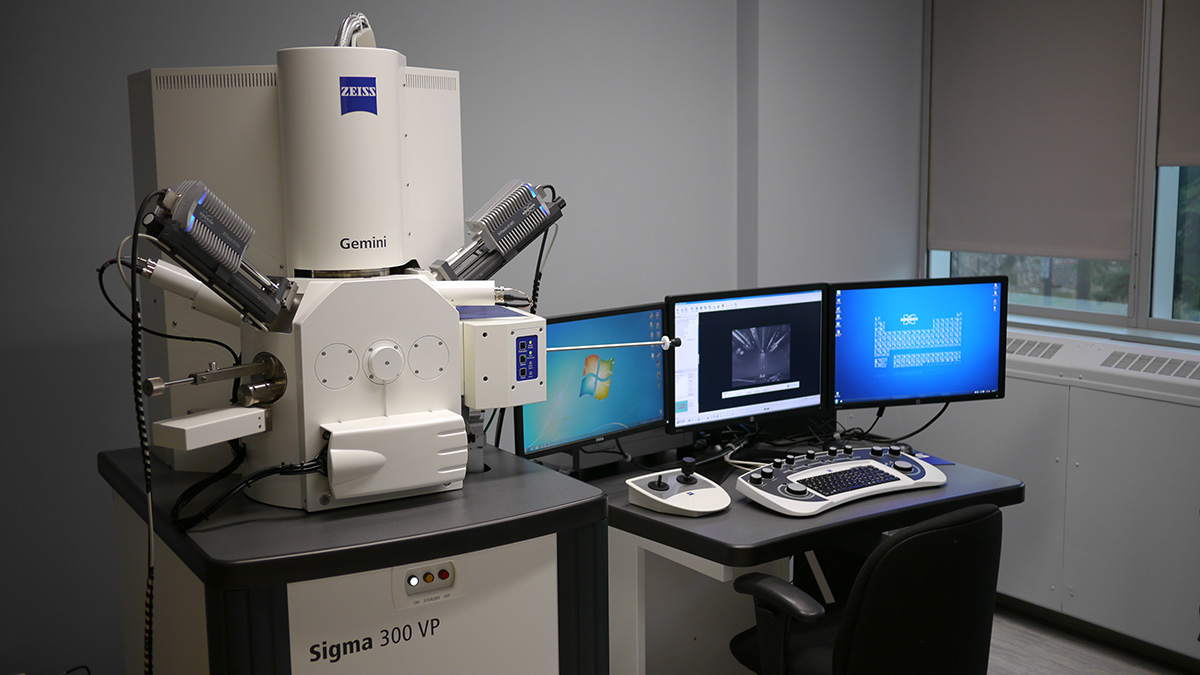
Zeiss Sigma Field Emission SEM operates in both high vacuum and variable pressure modes with a resolution of ~10 nm. It is equipped with secondary and backscattered electron detectors, an in-lens secondary electron detector, a cathodoluminescence (CL) detector, and a Bruker energy dispersive X-ray spectroscopy (EDS) system with dual silicon drift detectors each with an area of 60 mm2 and a resolution of 123 eV. The Sigma FESEM is technician operated; U of A users may also be trained to operate this SEM independently.
Zeiss EVO LS15 EP-SEM
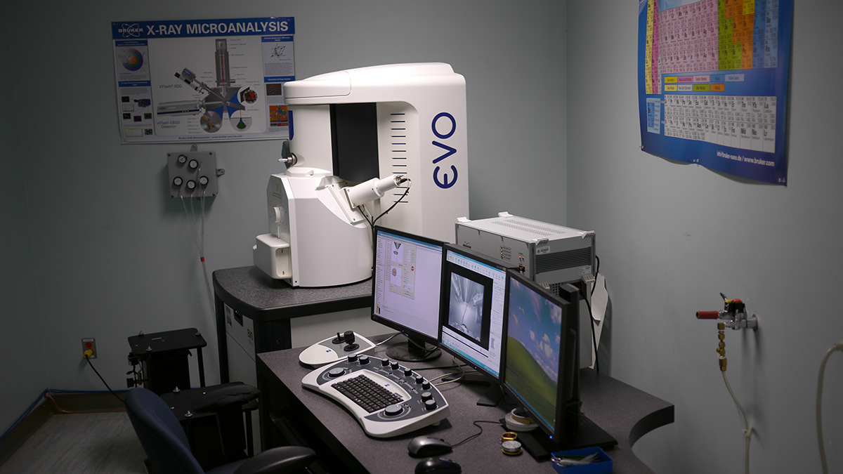
Zeiss EVO SEM with LaB6 electron source has a resolution of ~100 nm. It is equipped with a Bruker energy dispersive X-ray spectroscopy (EDS) system with a silicon drift detector with a resolution of 123 eV and a 10 mm2 window area. It is also able to operate in both variable pressure and extended pressure (environmental) modes. It is equipped with a cold stage and in environmental mode is able to image hydrated samples. This instrument is technician operated.
Sample Coating and Preparation
Conductive coatings of gold or carbon may be deposited using a Nanotek SEMprep 2 sputter coater or Leica EM SCD005 evaporative carbon coater. Samples may be prepared for imaging using a Bal-Tec CPD 030 critical point dryer.
For appointments or additional information e-mail eassem@ualberta.ca